
www.magazine-industry-usa.com
22
'26
Written on Modified on
ISRL USA and AIIP to Build Domestic Semiconductor Subfab Facility
The partners will launch a purpose-built subfab R&D platform providing a shared infrastructure environment for manufacturers to validate sustainable manufacturing technologies and workforce development programs while significantly reducing individual capital costs.
bodewellgroup.com
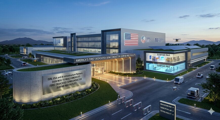
International SubFAB Research Labs (ISRL USA) and AI Infrastructure Partners (AIIP) have entered a memorandum of understanding to develop the first purpose-built R&D facility in the United States specifically for semiconductor subfab infrastructure. While traditional research centers focus on the cleanroom floor, this collaboration introduces a unique, industry-neutral platform designed to solve the scaling and sustainability challenges that private pilot lines and existing facilities cannot address alone. By providing a shared Infrastructure-as-a-Service (IaaS) model, the facility differentiates itself from high-cost proprietary labs, offering a cost-effective environment for validating next-generation abatement and materials reclaim technologies.
Solving the Subfab Innovation Gap
The subfab serves as the essential layer beneath the cleanroom, managing vacuum pumping, gas abatement, and chemical waste. Despite being the primary driver of the semiconductor industry’s environmental footprint, the subfab has historically lacked dedicated research infrastructure, forcing chipmakers like TSMC, Intel, and Micron to pursue net-zero targets without a centralized validation platform. This new facility closes that gap by replicating high-volume manufacturing conditions for legacy and leading-edge processes. It allows independent device manufacturers, foundries, and OEMs to conduct IP-protected research at a fraction of the $100 million investment typically required for private infrastructure.
A Collaborative Infrastructure-as-a-Service Model
Under the agreement, AIIP will oversee the design, construction, and ownership of the physical infrastructure, while ISRL USA manages technical operations and research programs. The partnership creates an accessible entry point for stakeholders across the supply chain to generate compliance-ready data and validate equipment in a pre-competitive environment. This model lowers the capital burden for individual participants and is structured to qualify for CHIPS Act incentives and international funding programs. With site selection currently underway, the facility aims for operational readiness within 12 months of funding, establishing a new physical backbone for American semiconductor manufacturing resilience.
Edited by Evgeny Churilov, Induportals Media - Adapted by AI.
www.bodewellgroup.com
