
www.magazine-industry-usa.com
01
'26
Written on Modified on
PECVD SiCN System Implementation for Semiconductor Process Control
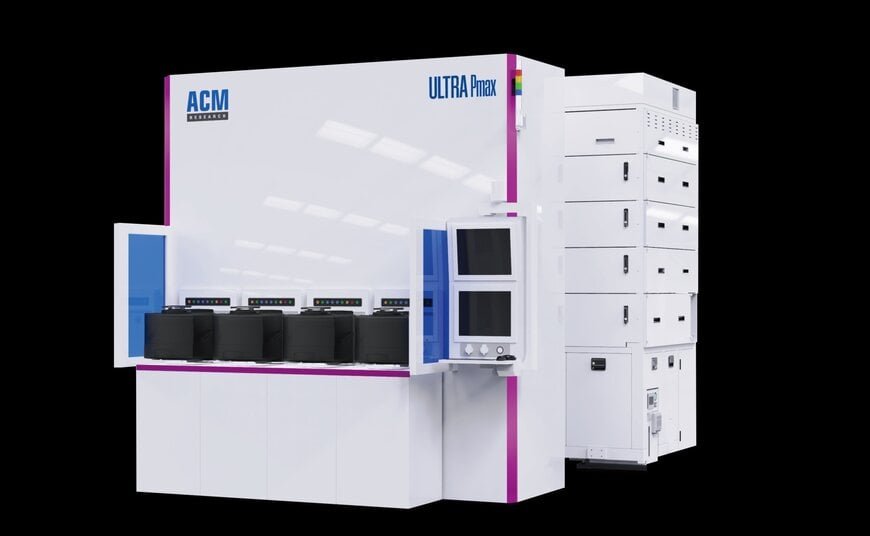
ACM Research installs a multi-station deposition architecture at a manufacturing site to improve film uniformity and stability in advanced semiconductor processing.
www.isrlusa.com
As logic device scaling continues below the 55 nm node, manufacturing processes become increasingly sensitive to interface defects and particle contamination. Back-end-of-line operations, such as copper interconnect formation, demand precise control over the thickness and composition of diffusion barriers and etch stop layers. Silicon carbonitride films are utilized for these applications due to their dielectric properties and high resistance to metal ion diffusion.
Technical Challenges in Thin-Film Deposition
Conventional plasma-enhanced chemical vapor deposition systems frequently utilize a single-station architecture. This configuration can limit the degree of control over intra-wafer uniformity and plasma distribution. In high-density integration environments, plasma-induced variability often leads to deviations in thin-film stacks, which can negatively impact the electrical performance of the finished semiconductor device.
Architectural Solution and Mechanism
To address these limitations, a deposition system was developed utilizing a three-station rotating configuration within a single reaction chamber. The process segments the total film thickness across three separate stations, which allows for controlled interface formation and stabilized gas flow dynamics across the wafer surface. Each station is equipped with an independent radio frequency source under a localized control scheme. This arrangement enables precise adjustment of plasma power, ensuring consistent ion energy distribution and improving process repeatability across the entire wafer.
System Validation and Site Integration
The implementation followed a validation phase at a laboratory in Lingang, where the system was tested against specific film uniformity and adhesion strength parameters. Following these tests, the equipment was delivered and installed at a semiconductor manufacturing facility. The integration process focused on verifying compatibility with existing automated wafer handling systems and aligning the deposition sequences with established fabrication workflows.
Process Stability and Reliability Outcomes
The multi-station approach provides a wider process window for thin-film deposition by isolating plasma control variables. This method reduces defect density and enhances the reproducibility of films used in copper oxidation reduction and etch stop layer formation. In advanced packaging, the resulting high-density silicon carbonitride films improve bonding integrity and long-term interconnect reliability, which are critical for the mechanical and electrical stability of heterogeneous integration architectures.
Edited by an industrial journalist, Lekshman Ramdas, with AI assistance.
www.isrlusa.com
